

Intace Biofoam
Intrinsically Conductive ESD Safe Semiconductor Packaging
Eliminating Longstanding Tradeoffs in Conductive Packaging Materials
Semiconductor and electronics systems are becoming smaller, more powerful, and increasingly sensitive to electrostatic discharge. As performance demands rise, even small limitations in packaging materials can affect reliability, contamination risk, and supply chain resilience.
Intace Biofoam is the first demonstration of Intace’s advanced polymer engineering technology, showing how functionality can be engineered directly into materials rather than relying on conventional additive based systems.
Designed for semiconductor and electronics packaging, Intace Biofoam delivers stable electrostatic protection without conductive fillers, carbon additives, or mineral based agents traditionally used in ESD safe foams. Instead, conductivity is engineered directly into the material system through a proprietary molecular level approach, enabling cleaner, more consistent, and high performance packaging materials for increasingly sensitive electronic components.

Why Semiconductor Packaging Needs a New Material Pathway
Conventional ESD safe foams often rely on petrochemical materials combined with conductive fillers to achieve electrostatic protection. While effective, these systems can introduce longstanding tradeoffs in contamination risk, conductivity consistency, mechanical performance, material complexity, and end of life impact.
As semiconductor systems become increasingly sensitive, these limitations become harder to tolerate. Even small variations in electrostatic stability or particle contamination can have outsized consequences across manufacturing, transport, and storage.
Intace Biofoam is designed to take a fundamentally different approach by engineering conductivity directly into the material system, rather than relying on conventional additive based methods.

1. Conductivity Without Conductive Fillers
For decades, conductive packaging materials have depended on carbon particles, conductive fillers, or mineral based additives to function, approaches that often introduce compromises in contamination risk, material consistency, electrostatic stability, and long term performance.
Intace Biofoam removes the need for conventional conductive agents by engineering conductivity directly into the material system itself, enabling electrostatic protection through the material rather than added particles.2. Cleaner and Lower Contamination Risk
Designed to reduce particle shedding, dusting, and contamination risks associated with additive based conductive foams, an increasingly important challenge for sensitive semiconductor and electronics components
2. Built for the Next Era of Semiconductor Hardware
As semiconductor systems become smaller, faster, and increasingly sensitive, tolerance for electrostatic instability, contamination, and material inconsistency continues to shrink.
Intace Biofoam is designed for environments where even small material limitations can become reliability challenges across manufacturing, handling, transport, and storage.
3. Cleaner by Design
Without conductive particles, carbon additives, or mineral based agents, Intace Biofoam is designed to reduce dusting, shedding, and contamination risks increasingly important for advanced semiconductor and electronics manufacturing.
4. Breaking Longstanding Tradeoffs of Conductive Materials
Traditional conductive foams often force compromises between electrostatic performance, cleanliness, mechanical behaviour, cost, and sustainability.
Intace Biofoam is designed to challenge these assumptions through a fundamentally different material engineering approach.
5. Built for More Resilient Supply Chains
Created from bio based inputs and designed for demanding industrial environments, Intace Biofoam provides a pathway toward lower dependency material systems for advanced semiconductor and electronics supply chains.
What Becomes Possible
Built for Semiconductor and Electronics Workflows
Intace Biofoam is being developed to integrate with existing semiconductor and electronics packaging workflows, reducing barriers to adoption while meeting increasingly demanding performance requirements.
Current application areas include:
Semiconductor packaging and transport
PCB and sensitive component handling
ESD safe storage and protection
High value electronics and advanced modules
We work closely with early industry partners to validate performance, manufacturing compatibility, and alignment with evolving technical requirements and industry standards.
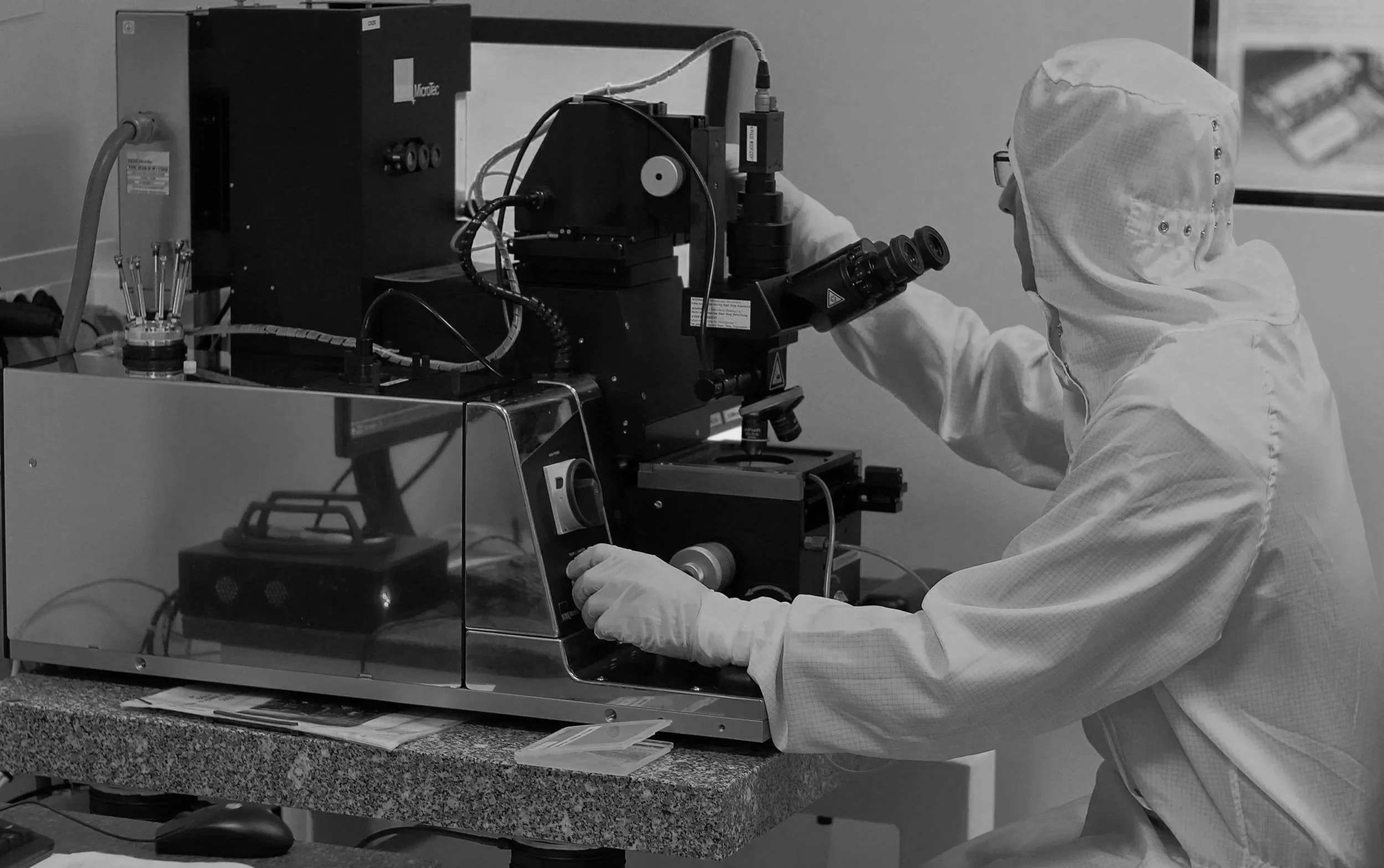
Intace is working with industry partners to advance Intace Biofoam toward real world deployment in semiconductor and electronics environments.
As performance demands continue to rise, we are focused on validating the material for increasingly demanding applications and industrial requirements.
We welcome conversations with partners interested in shaping the future of semiconductor and electronics materials.